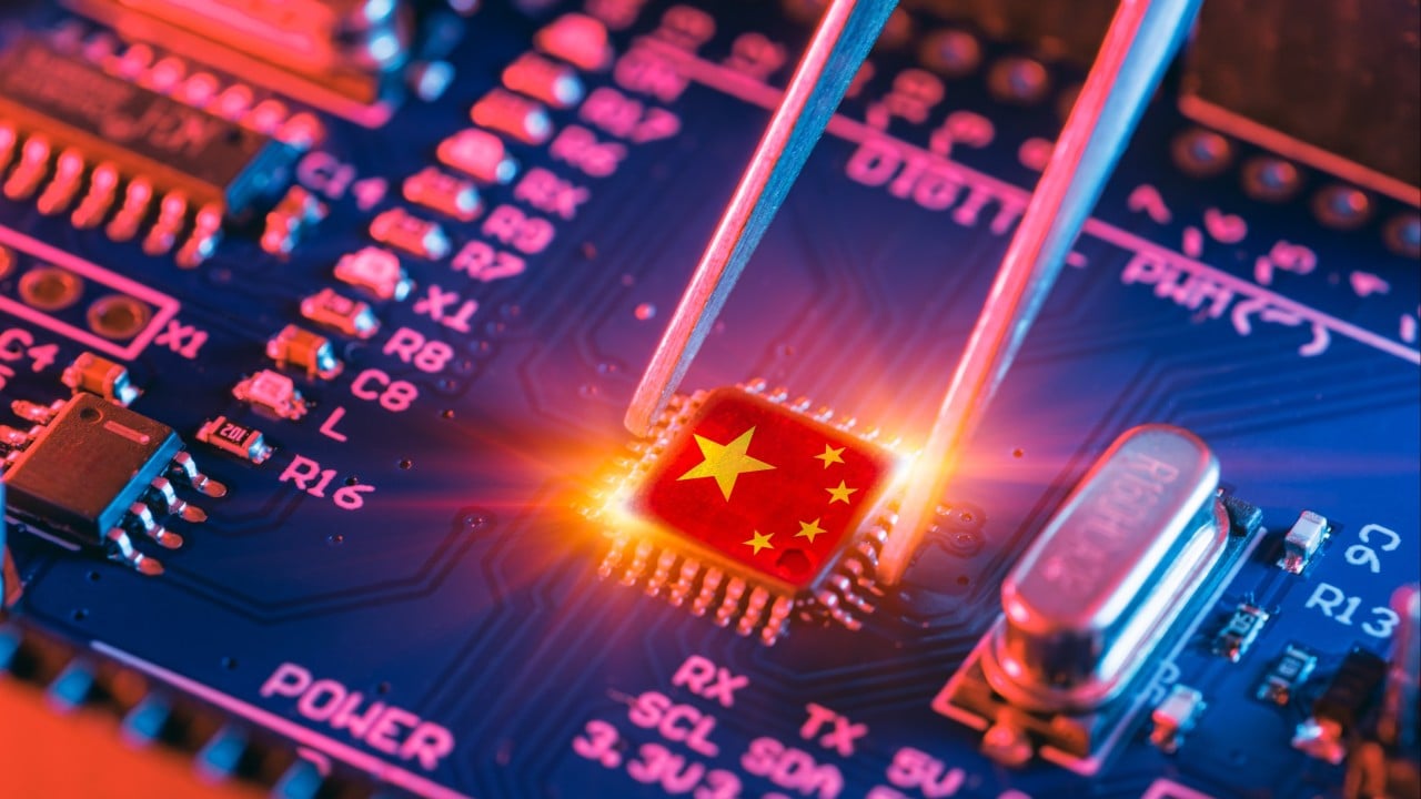
Washington intended its sweeping export controls to starve the Chinese artificial intelligence sector of computing power. By severing access to leading merchant silicon from American designers, policy architects expected to freeze domestic progress. Instead, the restrictions triggered a structural overhaul that is permanently reshaping the global semiconductor trade. Chinese tech companies are not giving up on high-performance computing. They are radically redesigning their architectures, supply chains, and silicon strategies to bypass Western roadblocks entirely. The result is an emerging, self-contained tech ecosystem that relies on alternative manufacturing methods and domestic alternatives to establish long-term self-sufficiency.
The Yield Illusion and the Deep Duplication Trap
The primary flaw in the initial Western sanctions strategy was an over-reliance on lithography limits as a permanent barrier. Analysts confidently asserted that without extreme ultraviolet lithography equipment from Europe, domestic foundries could never produce silicon efficient enough to challenge Western accelerators. Meanwhile, you can find other stories here: The Real Reason Washington Just Plugged the Billion Dollar Global AI Leak.
Observable realities in Asian manufacturing facilities have broken that thesis. Domestic fabrication plants have pushed deep ultraviolet immersion lithography far past its intended theoretical limits. By employing aggressive multi-patterning techniques, Semiconductor Manufacturing International Corporation successfully scaled its seven-nanometer process node.
The strategy is commercially inefficient, but geopolitical survival operates on a different balance sheet. Multi-patterning requires passing a silicon wafer through lithography machines multiple times to etch increasingly fine features. Every additional exposure layer increases the probability of a microscopic defect, causing chip yields to plummet. To see the full picture, check out the detailed report by Gizmodo.
Standard Single-Exposure Node:
[Wafer] ---> [Single Lithography Pass] ---> High Yield (85-90%)

Domestic Multi-Patterning Node:
[Wafer] ---> [Pass 1] ---> [Pass 2] ---> [Pass 3] ---> Low Yield (30-40%)
Industry intelligence indicates that early runs of these processors suffered from yields below forty percent. In a normal market, a sixty percent scrap rate represents commercial suicide. When backed by sovereign capital injections, however, the financial calculation changes. The state effectively absorbs the cost of the wasted silicon, ensuring that domestic enterprises receive functional hardware regardless of production costs.
This high-overhead manufacturing model has already yielded commercial hardware. Major domestic tech firms have largely abandoned attempts to source restricted American hardware through grey markets. They are shifting production workloads to local silicon alternatives instead.
Huawei has emerged as the clear leader in this domestic shift. Its Ascend series of processors has become the default architecture for state-backed data centers and local cloud providers. The company is actively doubling its seven-nanometer manufacturing capacity, building out a predictable domestic pipeline that operates completely independently of Western supply lines.
Architecting Around the Lithography Wall
Because domestic foundries cannot easily shrink transistors further, engineering teams are focusing on architectural adjustments to boost performance. If a single chip cannot be made smaller, the alternative is to combine multiple chips into a single, cohesive processing unit.
This focus has accelerated domestic development of advanced packaging and advanced chiplet architectures. Instead of manufacturing a massive, complex processor on a single piece of silicon, designers break the system down into smaller, functional modules called chiplets. These individual components can be manufactured on mature, high-yield process nodes and then linked together on a high-speed substrate.
+-------------------------------------------------------+
|                      Silicon Carrier Substrate        |
|                                                       |
|  +-----------------+  +------------+  +------------+  |
|  |     Compute     |  | High Band  |  | High Band  |  |
|  |     Chiplet     |  |   Memory   |  |   Memory   |  |
|  |  (7nm Node)     |  |   (HBM)    |  |   (HBM)    |  |
|  +-----------------+  +------------+  +------------+  |
|           |                 |               |         |
|  ================== High-Speed Interconnect ========  |
+-------------------------------------------------------+
This structural shift introduces significant engineering hurdles:
- Interconnect Density: Splitting a processor across multiple dies requires thousands of microscopic connections running between them, requiring high-precision substrate manufacturing.
- Thermal Accumulation: Stacking components closely together creates concentrated thermal zones, necessitating advanced liquid cooling systems inside data centers.
- Latency Penalties: Data moving between physically separate pieces of silicon takes longer to travel than data moving across a single die, requiring sophisticated software optimization to hide the delay.
To overcome these latency issues, domestic software engineers are rewriting fundamental elements of the artificial intelligence stack. They are developing specialized compilers designed to treat these distributed hardware setups as single logical processors. This software layer optimizes how data moves across the chiplets, minimizing bottlenecks and ensuring that lower-yield domestic hardware can approximate the performance of integrated Western accelerators.
The Memory Breakthrough
An artificial intelligence processor is useless without rapid access to massive pools of data. For years, the lack of local high bandwidth memory stood as a critical weakness for domestic hardware initiatives. Global memory production was dominated by a tight trio of companies in South Korea and the United States, leaving domestic chip designers holding high-performance compute logic with no fast memory pipeline to feed it.
That reliance is beginning to crack. Changxin Memory Technologies has broken through the capital-intensive memory barrier, turning its first annual profit and reporting massive revenue jumps. The firm has shifted from historical losses to a highly profitable operation, driven by soaring domestic demand for modern memory architectures.
+---------------------------------------------------------+
|             Domestic Memory Revenue Surge               |
+-------------------------+-------------------------------+
| Period                  | Revenue                       |
+-------------------------+-------------------------------+
| Full Year 2024          | Net Loss State                |
| First Quarter 2026      | 50.8 Billion Yuan             |
| First Half 2026 (Proj.) | 110.0 - 120.0 Billion Yuan    |
+-------------------------+-------------------------------+
This financial turnaround reflects a major strategic shift. Domestic memory factories are rapidly scaling production of high-end memory formats like DDR5 and specialized low-power variants. More importantly, they have begun ramping up volume production of high bandwidth memory.
By utilizing customized die structures, domestic memory makers are delivering the dense memory stacks required by modern AI processors. While these products currently require slightly larger physical footprints than their Western counterparts, they deliver the necessary data throughput. This gives domestic chip designers a completely local memory supply chain for the first time.
The Illusion of Containment
The shifting regulatory approach in Washington highlights the immense difficulty of isolating a deeply interconnected global industry. For a time, a regulatory gap allowed overseas subsidiaries of Chinese companies to purchase high-end American processors without requiring specific export licenses. These entities operated outside mainland borders, frequently utilizing data hubs in Southeast Asian nations like Malaysia to build out robust infrastructure pipelines.
Industry tracking suggests that hundreds of thousands of advanced processors moved through these international channels over a twelve-month period. When independent policy reviews exposed the scale of this hardware movement, regulatory bodies rushed out emergency weekend updates to close the loophole. The updated guidance extended license requirements to any company headquartered in China, regardless of where its physical purchasing offices are located.
Yet each new restriction simply uncovers another layer of operational reality. While the rules now cover overseas subsidiaries, they drop strict due diligence mandates for international foundries. This leaves a complex network of front companies and intermediaries free to order custom silicon, mask true ownership structures, and keep hardware flowing through indirect channels.
Furthermore, these updated rules only restrict future shipments. They do not require international data hubs to stop using existing hardware, nor do they halt ongoing maintenance and support services for systems already in place. The hardware already deployed overseas continues to run production workloads, giving domestic enterprises continued access to top-tier compute capabilities while they finalize their internal supply chains.
Redesigning the Software Ecosystem
Building functional silicon is only half the battle. The true strength of Western dominance lies in the deeply entrenched software ecosystem that developers use to write, optimize, and deploy artificial intelligence models. This proprietary software platform functions as an industry standard; virtually every major AI model is optimized to run on it.
To break this software dependency, domestic tech giants are collaborating on a shared software layer designed to abstract away the underlying hardware. This open software architecture allows developers to write code once and run it on a variety of domestic processors without extensive rewrites.
The Migration Pipeline
- Model Ingestion: A standard artificial intelligence model trained on Western frameworks is passed to a domestic compiler.
- Kernel Translation: The compiler translates proprietary operations into open-source equivalents optimized for local silicon architectures.
- Dynamic Graph Optimization: The software analyzes the model structure, automatically breaking up workloads to match the chiplet layout of domestic hardware.
- Hardware Execution: The optimized instructions run directly on local processors, minimizing execution bottlenecks.
This unified software approach significantly lowers the operational barrier for local companies looking to migrate away from Western platforms. Instead of being locked into a single vendor ecosystem, enterprise buyers can source hardware from multiple local suppliers, knowing their existing models will run without requiring complete software redesigns.
The Fragmented Global Supply Chain
The aggressive drive for technological self-reliance is fracturing what was once a highly integrated global market. As domestic tech firms pull back from international vendors to support local suppliers, they create a completely separate technological stack. This split extends far beyond compute logic and memory chips, altering the demand dynamics for fundamental components across the entire global infrastructure pipeline.
                  Global Technology Splitting

      Western Stack                  Domestic Stack
+-----------------------+      +-----------------------+
|  Integrated Silicon   |      |  Chiplet Assemblies   |
|  EUV Lithography      |      |  Multi-Patterning DUV |
|  Western Monopolies   |      |  State-Backed Foundries|
|  Standard Hardware    |      |  Liquid-Cooled Hubs   |
+-----------------------+      +-----------------------+
This structural shift is driving extreme demand variations in often overlooked areas. The push to link distributed data hubs has triggered acute shortages in optical communications infrastructure. Critical components like specialized optical fibers, pluggable transceivers, and indium phosphide substrates have seen massive price increases as both Western and domestic infrastructure rollouts scramble for supply.
Simultaneously, international buyout groups and private equity firms are rapidly divesting from data infrastructure assets inside China. Rising geopolitical risks and tightening data security laws have turned these capital-intensive investments into significant political liabilities. These assets are being steadily acquired by domestic, state-backed buyers, shifting ownership of critical digital infrastructure firmly into local hands.
The current landscape makes one reality undeniably clear: export controls did not halt technological progression. They simply shifted the playing field, forcing the development of a highly resourceful, heavily subsidized, and completely independent silicon supply chain. Washington may have succeeded in cutting ties with its leading tech rival, but in doing so, it forced the creation of a permanent, self-contained competitor.